SEMICONDUCTORS have conductivity, more than of insulators and less than conductors.
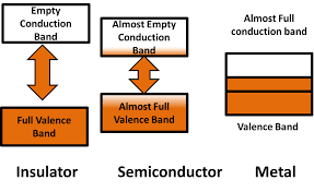
Valence Band is graphical depiction of Energy of valence Band
Conduction Band is lowest value of electron, if it is free to conduct electricity
Gap between the lowest line of Conduction Band and Upper line of Valence Band is called Forbidden Energy Gap
FEG < 1 eV is conductor
1< FEG < 3 eV SEMICONDUCTOR
FEG >3 3V INSULATOR
Intrinsic Semiconductor: The pure semiconductors in which the electrical conductivity is totally governed by the electrons excited from the valence band to the conduction band and in which no impurity atoms are added to increase their conductivity are called intrinsic semiconductors and their conductivity is called intrinsic conductivity. Electrical conduction in pure semiconductors occurs by means of electron-hole pairs. In an intrinsic semiconductor,
ne = nh = ni
where ne = the free electron density in conduction band, nh = the hole density in valence band, and ni = the intrinsic carrier concentration.
Extrinsic Semiconductors. A Semiconductor doped with suitable impurity atoms so as to increase its conductivity is called an extrinsic semiconductor. Extrinsic semiconductors are of two types:
(i) n-type semiconductors. And (ii) p-type semiconductors.
n-type semiconductors. The pentavalent impurity atoms are called donors because they donate electrons to the host crystal and the semiconductor doped with donors is called n-type semiconductor. In n-type semiconductors, electrons are the majority charge carriers and holes are the minority charge carriers. Thus ne = Nd + nh
here Nd = Number density of donor atoms
p-type semiconductors. The trivalent impurity atoms are called acceptors because they create holes which can accept electrons from the nearby bonds. A semiconductor doped with acceptor type impurities is called a p-type semiconductor. In p-type semiconductor, holes are the majority carriers and electrons are the minority charge carriers Thus nh = Nd + ne
here Na = Number density of acceptor atoms
Holes. The vacancy or absence of electron in the bond of a covalently bonded crystal is called a hole. A hole serves as a positive charge carrier.
Mobility. The drift velocity acquired by a charge carrier in a unit electric field is called its electrical mobility and is denoted by m. Mathematically
The mobility of an electron in the conduction band is greater than that of the hole (or electron) in the valence band.
Electrical conductivity of a Semiconductor. If a potential difference V is applied across a conductor of length L and area of cross-section A, then the total current I through it is given by I= eA (neve + nh vh)
where ne and nh are the electron and hole densities, and ve and vh are their drift velocities, respectively. If me and mh are the electron and hole mobilities, then the conductivity of the semiconductor will be σ = e (neme + nhmh) The conductivity of an intrinsic semiconductor increases exponentially with temperature.
Forward and Reverse Biasing of a pn-junction. If the positive terminal of a battery is connected to the p-side and the negative terminal to the n-side, then the pn-junction is said to be forward biased. Both electrons and holes move towards the junction. A current, called forward current, flows across the junction. Thus a pn-junction offers a low resistance when it is forward biased.
If the positive terminal of a battery is connected to the n-side and negative terminal to the p-side, then pn-junction is said to be reverse biased. The majority charge carriers move away from the junction. The potential barrier offers high resistance during the reverse bias. However, due to the minority charge carriers a small current, called reverse or leakage current flows in the opposite direction. Thus junction diode has almost a unidirectional flow of current.
Types and Uses of Diode
Normal PN diode as rectifier.
Rectifier is a device used to convert AC voltage to DC Voltage. Full wave and Half wave.
In full wave the output frequency is double the input, while in half wave the output frequency same as input.
Zener used as voltage regulator, works in reverse bias.
Optoelectronic junction devices
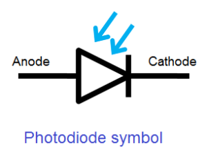
(i) Photodiodes used for detecting optical signal (photodetectors). Used to detect signals, used in reverse Bias
(ii) Light emitting diodes (LED) which convert electrical energy into light. It emits light, Used in Forward Bias
(iii) Photovoltaic devices which convert optical radiation into electricity (solar cells). It is NOT biased. It generates electricity.
DOWNLOAD NOTES HERE
Action of a transistor. When the emitter-base junction of an npn-transistor is forward biased, the electrons are pushed towards the base. As the base region is very thin and lightly doped, most of the electrons cross over to the reverse biased collector. Since few electrons and holes always recombine in the base region, so the collector current Ic is always slightly less then emitter current IE.
IE = IC + IB , where IB is the base current
![]()
In every type of transistor, the EMITTER BASE junction is forward biased and COLLECTOR BASE is Reverse Biased. And Input in CE and CB configuration is BASE EMITTER junction where the input resistance is low and output from collector where Resistance is Very High.
Three Configurations of a Transistor. A transistor can be used in one of the following three configurations:
(i) Common-base (CB) circuit.
(ii) Common-emitter (CE) circuit.
(iii) Common-collector (CC) circuit.
Logic Gate. A logic gate is a digital circuit that has one or more inputs but only one output. It follows a logical relationship between input and output voltage.
Truth Table. This table shows all possible input combination and the corresponding output for a logic gate.
Boolean Expression. It is a shorthand method of describing the function of a logic gate in the form of an equation or an expression. It also relates all possible combination of the inputs of a logic gate to the corresponding outputs.
Positive and Negative Logic. If in a system, the higher voltage level represents 1 and the lower voltage level represent 0, the system is called a positive logic. If the higher voltage represents 0 and the lower voltage level represents 1, then the system is called a negative logic.
OR Gate. An OR gate can have any number of inputs but only one output. It gives higher output (1) if either input A or B or both are high (1), otherwise the output is low (0).
A + B = Y, which is read as ‘A or B equals Y’.
AND gate. An AND gate can have any number of inputs but only one output. It gives a high output (1) if inputs A and B are both high (1), or else the output is low (0). It is described by the Boolean expression. A.B = Y, which is read as ‘A and B equals Y’.
NOT Gate. A NOT gate is the simplest gate, with one input and one output. It gives as high output (1) if the input A is low (0), and vice versa.Whatever the input is, the NOT gate inverts it. It is described by the Boolean expression: which is read as ‘not A equal Y’.
![]()